


October 3, 2019 -- According to a new report from Strategic Directions International (SDI), the total market for electron microscopy instrumentation was in excess of $2.5 billion in 2018 and is expected to reach nearly $3.4 billion by 2023.
Microscopic techniques have revolutionized our understanding of the universe, both for the life sciences as well as for the basic understanding of matter and materials in the physical sciences and industry. While optical microscopy techniques provide a wealth of information, when researchers turn to smaller and smaller features, whether cellular components or cutting-edge electronics, only electron microscopy can deliver the resolution required to achieve these goals. The market for these instruments remains a vital one, with a very broad array of applications in both industry and academia.
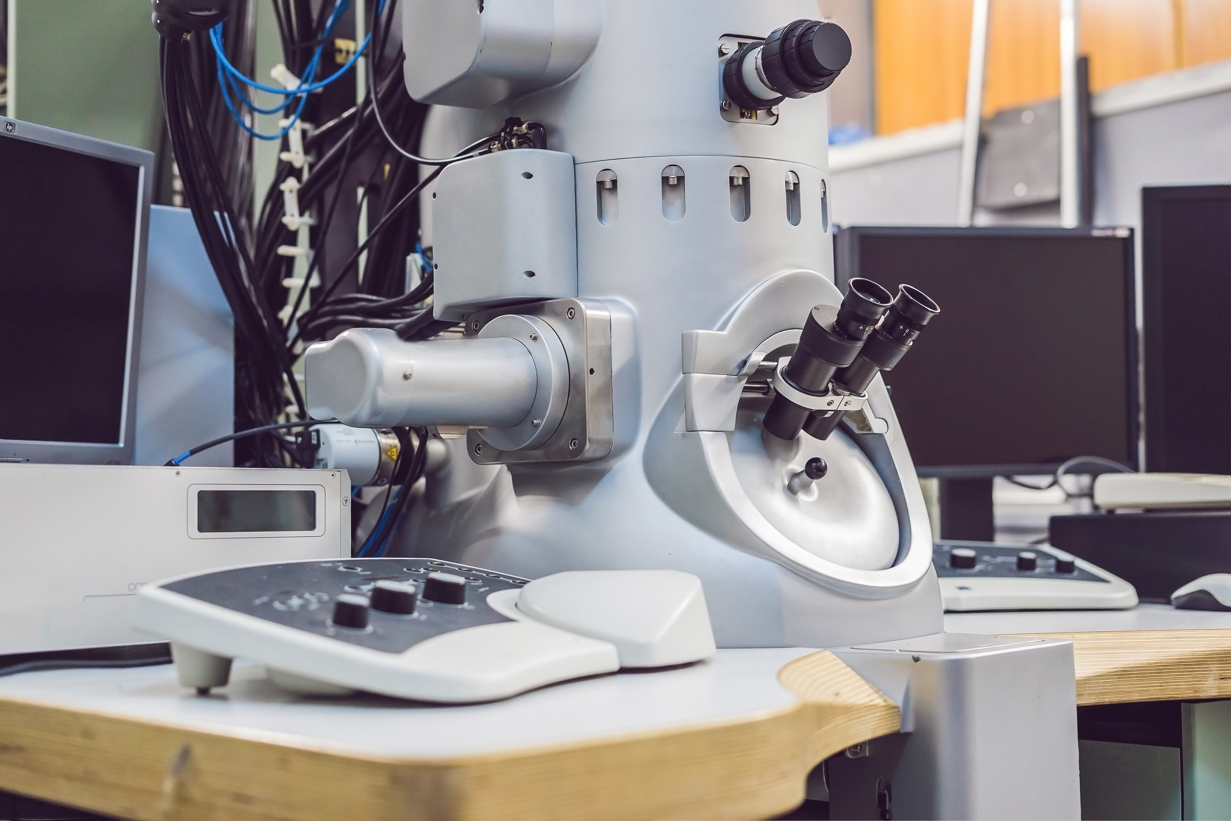
Electron microscopy has long been a staple microscopy technology, especially for characterization in the semiconductor industry as well as for other materials. However, new technological innovations combined with emerging industries have opened the door to new applications where electron microscopy is likely to be of significant demand for the long-term. According to SDi's recent The 2019 Market for Electron Microscopy report, the electron microscopy market will grow 6% over the next five years.
There are several areas where the trend can be seen:
Preserving Structural Biology Samples. Historically, there have been many challenges with imaging biological samples via electron microscopy due to the harsh conditions a sample must endure. High vacuum sample chamber environments, the requirement for conductive samples, and the bombardment of electrons on a sample have long been considered serious limitations for biology research.
Today, however, structural biology is relying more and more on electron microscopy to continue new discoveries and advancements. Cryo-electron microscopy, in particular, is especially well-suited for bioimaging due to much less destructive sample conditions. In cryo-EM samples are essentially frozen in a specialized way in order to preserve the natural state of the biosample. In addition, other innovations such as lower vacuum requirements and advances in image processing software have optimized conditions for structural biology applications. The key is that electron microscopy and cryo-EM are bound to become even better adapted for structural biology applications as the technology develops. This will be significant because biosamples, which traditionally were only able to be characterized using light or fluorescence microscopy, can now be viewed at much higher magnification than ever before, opening the door to new insights and discoveries.
Gaining visibility on Nanotechnology. Nanotechnology-based advances will be observed in virtually every industry over the next decade. From cancer therapeutics, to implant coatings that improve biocompatibility, to "smart" materials that adapt to their environment, nanotech products are likely to only accelerate in diversity and application. Nanotech and electron microscopy will go hand-in-hand due to the need to see and characterize smaller and smaller features. Tabletop electron microscopy systems enable the technology to be more accessible to end-users via reduced price points. It is likely that more and more industries that did not traditionally need such magnification will require electron microscopy characterization due to the rapid emergence of nanotechnology-based products.
Submillimeter Systems. These are electronic and/or mechanical systems that are submillimeter in scale. MEMS are manufactured using the same techniques long employed by the semiconductor industry yet they have much different applications and end markets. One of the most commercially successful examples of MEMS are airbag sensors that exist in automobiles. However, MEMS are becoming even more diverse such as in the form of microfluidic platforms for point-of-care diagnostics, advanced LED-chip displays, and even in micro-robotic surgery systems. Like semiconductors, MEMS will definitely demand high electron microscopy use for characterization throughout development and production.
To learn more about the specific products in the field of electron microscopy visit SDI's website and view "The 2019 Market for Electron Microscopy: The Future of Electron Optics and Microanalysis"
Copyright © 2019 scienceboard.net
Member Rewards
Earn points for contributing to market research. Redeem your points for merchandise, travel, or even to help your favorite charity.

Research Topics
Interact with an engaged, global community of your peers who come together to discuss their work and opportunities.
Conferences
Connect


